The functions of this lab are to provide (1) experimental modules for the Introduction to Microfabrication course (PHYS/ECE/BENG/MAE 5700), and (2) processes to support research across campus.
Lithography
Photolithography begins with spin-coating of HMDS and photoresist on 4-in wafers or pieces followed by a soft-bake. Exposure will be performed by an ABM mask aligner with a broadband mercury lamp. After a post-exposure bake, manual development is conducted in a dish followed by DI water rinse and spin-dry. Linewidth as low as 800 nm can be achieved.
E-beam lithography on pieces can be conducted by a NPGS attachment to a Quanta 650 SEM to achieve a minimum linewidth of 50 nm.
Thin-film Deposition
Metal and dielectric thin-film deposition on 4-in wafers and pieces can be conducted by an AJA Orion-5 Sputtering System. Available targets include Au, Ag, Al, Co, Cr, Cu, Fe, Mo, Ni, Pt, Si, Ta, Ti, W, BN, SiO2, TiO2, Si3N4, ITO, and Al2O3. Single layer and bilayer liftoff can be performed subsequently.
High-melting point, high-purity, or more directional deposition processes can be conducted by an AJA e-beam/thermal deposition system where pallets of SiO2, Ti, Cu, Ag, Al are currently available.
Etching
Aqueous HF, KOH, Al-etchant, and Cu-etchant are available to perform wet etching on SiO2, Si, Al or Cu layers. Dry etching with gases such as O2, SF6 and CHF3 are available to etch photoresist, Si and SiO2 by a SAMCO RIE-1C reactive ion etch system.
Chemical Vapor Deposition
A 3”-bore, 34”-long, single zone, split tube furnace with computer-controlled mass-flow controllers and vacuum pumps can perform annealing at various ambient conditions and chemical vapor deposition via precursor gases. More than 400 runs of carbon nanotube growths were conducted in this system.
A 6”-bore, 53”-long, 3-zone, Lindburg/Blue tube furnace is also available for chemical vapor deposition on larger-sized samples. Currently it is fitted for thermal oxidation of Si pieces in a 2”-diameter process tube.
Characterization
Resistivity can be measured by a Signatone 4-point probe. Thickness of transparent thin films can be measured by a Nanospec 3000 reflectometer. General film thickness can be measured by a Tencor Alpha-step 500 profilometer. Optical microscopy can be conducted by an Olympus BX51 compound microscope. Surface topography can be characterized by a Park System XE-100 atomic force
microscope. Grain orientation, elemental analysis, and surface morphology can be characterized by the Quanta 650 scanning electron microscope housed in the nearby Microscopy Core Facility.
Research Highlights: Carbon Nanotube Forest
Fabrication of Height-Modulated Carbon Nanotube Forests: Morphologies and Prospects for Broadband Absorption
Carbon Trends 4, 100040 (2021)
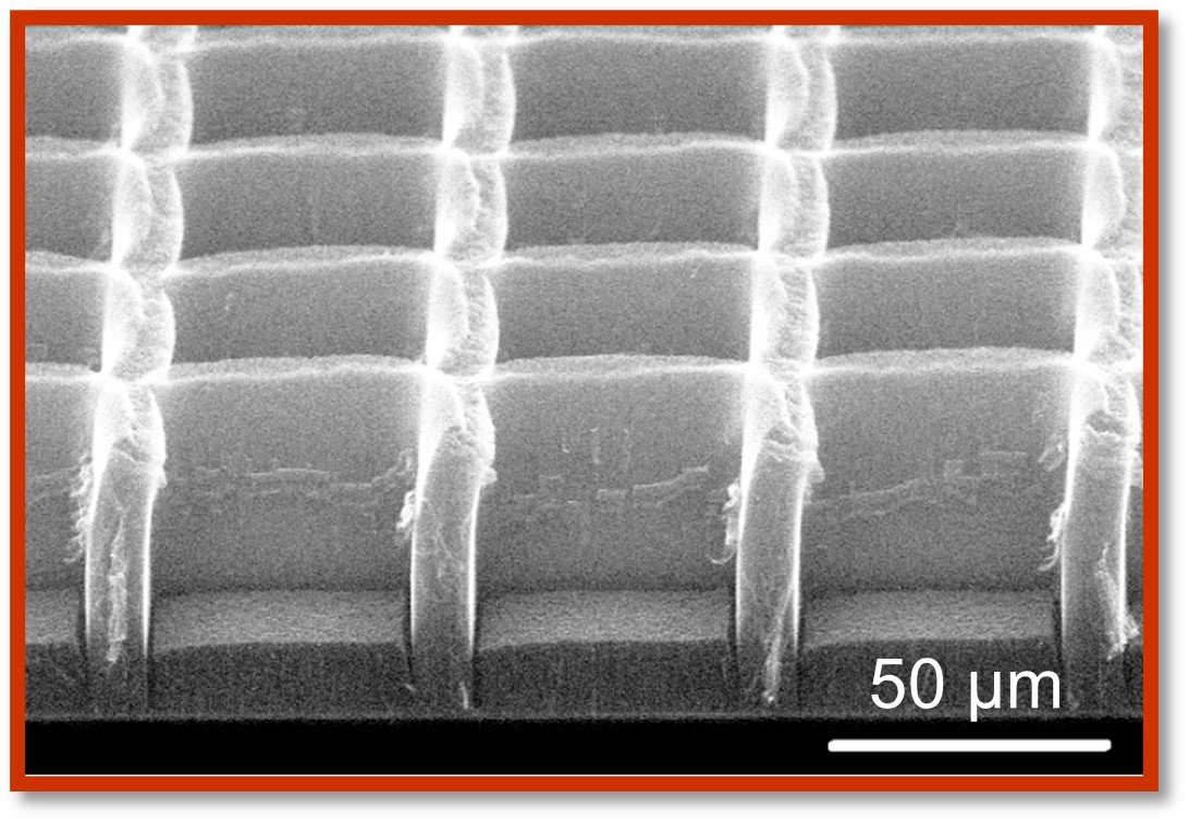
Fe and Fe/Co films as catalyst were deposited as patterns of grids and cell regions on a substrate, respectively. Due to the significant different growth rates of CNT forest on these catalyst particles, a patterned forest with 60-μm-tall forest on the grids and 15-μm-tall forest in the cells can be achieved. The objective of this research is to study the correlations between reflectance spectra and the geometry of modulation for broadband absorption.
Synthesis of High-Specific Volume Carbon Nanotube Structures for Gas-Phase Applications
Diamond & Related Materials 88, 230-236 (2018)
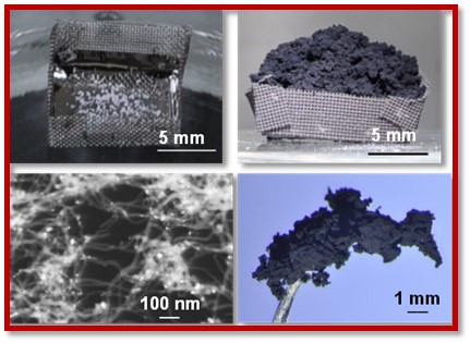
Multi-walled carbon nanotubes were nucleated and grown on alumina nanoparticles using a liquid precursor of ferrocene dissolved in xylene. Forces generated by CNT growth separated the alumina support clusters to result in a porous entangled structure with a 60-times gain in weight and a 1300-times gain in volume, compared to the original alumina particles. The resulting material has potential applications to support catalyst or adsorbent for gas-phase chemical processes including capturing CO2 from air.
Optical Reflection and Absorption of Carbon Nanotube Forest Films on Substrates
Journal of Applied Physics 118, 013106 (2015)
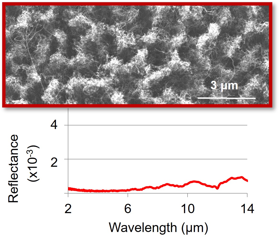
Surface interactions between Nb and Si at 700 ºC in an Ar/H2 ambient generate a corrugated substrate which leads to more Fe-nanoparticle formation in the valleys than on the mount. As a result, a random network of CNT forests can be created on Al/Nb/Si substrates. The forest height modulation allows longer wavelength light penetrating into the CNT structure and absorbed. With forest heights only 16-18 μm, the total reflectance is < 0.002 in the spectral range of 2-14 μm. This result indicates shorter and structured CNTs can be as effective as their longer unstructured counterparts for broadband light absorption.